
SPONSOR: Gratomic Inc. (TSX-V: GRAT) Advanced materials company focused on mine to market commercialization of graphite products, most notably high value graphene based components for a range of mass market products. Collaborating with Perpetuus, Gratomic will use Aukam graphite to manufacture graphene products for commercialization on an industrial scale. For More Info Click Here
A new technique to make ultra-flat, wrinkle-free films of graphene could pave the way for a host of applications, including graphene-based flexible electronics and high-frequency transistors. The technique works by introducing protons into the film as graphene is synthesized using chemical vapour deposition (CVD), and its inventors say that it might be extended to other two-dimensional materials such hexagonal boron nitride (h-BN) and the transition-metal dichalcogenides (TMDCs). It could also aid the development of hydrogen storage devices made from layered 2D structures.
Graphene – a 2D honeycomb of carbon atoms just one atom thick – boasts several unique electronic properties. In contrast to conventional semiconductors, which have an energy gap between the electron valence and conduction bands, graphene is a “zero-gap†semiconductor. This means its electron valence and conduction bands just touch each other. At the point of contact, the electrons move at near-ballistic speeds, and their behaviour is governed by the Dirac equation for relativistic electrons – hence the name “Dirac point†for this section of graphene’s band structure.
Linear defects
So far, this electronic behaviour has only been observed in small flakes of graphene that have been shaved off, or exfoliated, from samples of bulk graphite. These flakes are not big enough to be practical for electronic circuits, and although larger, wafer-sized graphene films can easily be produced via CVD, their electronic performance is not as good. This is because CVD-grown graphene, unlike the exfoliated type, contains grain boundaries, atomic vacancies, impurities and wrinkles. These defects act as centres off which electrons can scatter as they travel, thus degrading the material’s electronic properties.
CVD-produced graphene is prone to wrinkling because the graphene must adhere to the surface of a substrate as it grows. If the thermal expansion coefficient of the substrate does not match that of the graphene itself, a change in temperature can lead to linear defects – wrinkles – forming as the ensemble strives to release compressive strain.
Researchers have attempted to reduce wrinkling by performing CVD at low temperatures, using substrates with a similar thermal coefficient to that of graphene, and developing single-crystalline substrates. A team of researchers led by Libo Gao at China’s Nanjing University has now shown that reducing the interaction between graphene and its substrate might be a good, alternative, strategy.
Intercalating hydrogen molecules
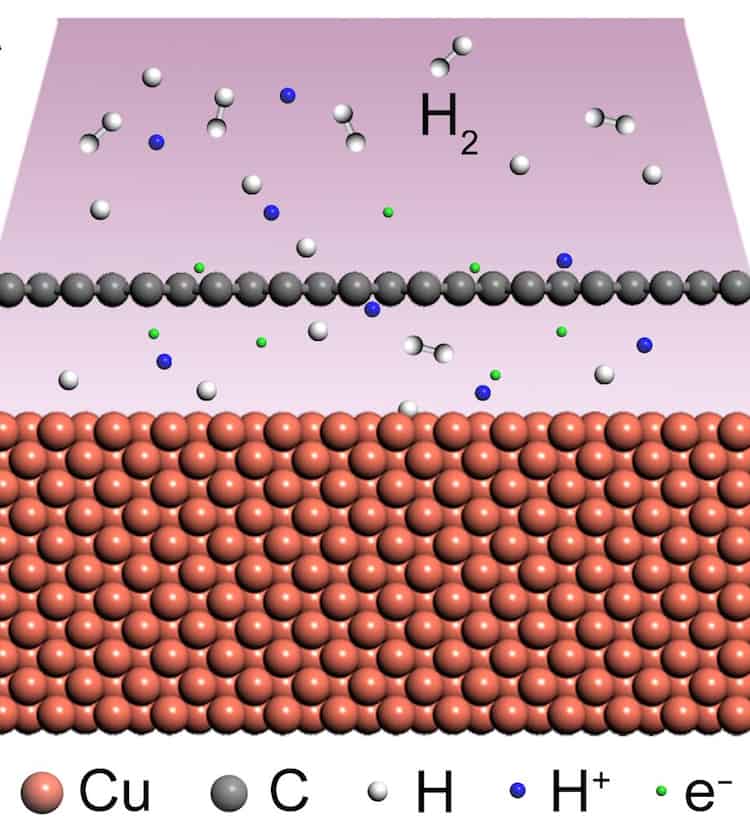
The Nanjing team began by introducing a plasma of protons – hydrogen ions – into the graphene’s growth chamber. During the CVD process, some of this hydrogen became intercalated between the graphene and its substrate, causing the two materials to decouple.
Gao and colleagues found that some of the wrinkles disappeared entirely from the graphene thanks to this proton penetration. They believe this is due to decreased van der Waals interactions between the carbon sheet and the substrate, as well as – possibly – an increase in the substrate’s distance from the growth surface thanks to the intercalation process.
High-quality bilayer graphene goes large
The researchers also found that the electronic band structure of their graphene films shows a V-shaped “Dirac cone†(representing the density of states around the Dirac point) similar to the one observed in exfoliated graphene. They argue that this proves the proton-assisted CVD-grown graphene is indeed decoupled from its substrate.
The technique, which is detailed in Nature, could be extended to grow ultra-flat versions of other 2D materials, such as h-BN and the TMDCs, Gao says. It might also make it possible to develop hydrogen storage devices made from these layered materials.
“The physical and electronic properties of our ultra-flat graphene films are homogenous on the large scale, which means they might now be used in higher-performance electronic and photoelectronic devices,†he tells Physics World.
Source:https://physicsworld.com/a/ultra-flat-graphene-goes-wrinkle-free/
Last modified: July 13, 2026