


SPONSOR: Gratomic Inc. (TSX-V: GRAT) Advanced materials company focused on mine to market commercialization of graphite products, most notably high value graphene based components for a range of mass market products. Collaborating with Perpetuus, Gratomic will use Aukam graphite to manufacture graphene products for commercialization on an industrial scale. For More Info Click Here

Graphene is only one-atom thick in its monolayer form and approximately 0.32 nanometers in the Z-axis. This means that the third dimension is eliminated, and it is classed as a 2D, all-surface material. Put into perspective, a stack of three million graphene sheets would only be 1 mm thick
Graphene in its monolayer form is the strongest material ever tested despite being extremely thin, a strength that comes in part from its flexibility which means it is also the most stretchable crystal material measured to date. It is also 97.7 percent transparent and has an extremely low permeability rate, with even helium atoms being unable to penetrate it.
Graphene also boasts the highest thermal conductivity ever recorded, standing at 10 times higher than copper. Further adding to its advantages as a material is the fact that it has the highest intrinsic electron mobility that is approximately 100 times greater than silicon. This property, in particular, has intrigued electronics applications for the last 15 years.
Engineered Properties Applications
Table 1. Graphene’s Properties and Associated Applications.
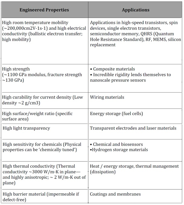
Source: Graphene Frontiers, Ruoff.
Altogether, these properties make graphene the latest “wonder material†in advanced materials science and technology. This has resulted in research on other 2D materials that are analogous to graphene, from hexagonal boron nitride (h-BN), Molybdenum Disulfide (MoS2), transition metal dichalcogenides (TMDCs) and black phosphorus, to silicene, germanene, and others.
The wider group of 2D materials is significant in relation to graphene as it exhibits a wider spectrum of electronic properties when compared to metals, semimetals, and semiconductors that all have different gaps in their energy bands, as well as insulators.
Additionally, combining the materials in this wider 2D group through layering results in heterostructures that possess unique physical properties of their own. This range of 2D materials and the heterostructures that can be formed when these 2D materials work in combination have a broad spectrum of applications, including electronics, optoelectronics, sensors, flexible and wearable devices, catalysis, and more.
This information has been sourced, reviewed and adapted from materials provided by The Graphene Council.
SOURCE: For more information on this source, please visit The Graphene Council.
Last modified: July 13, 2026


 as AI-Powered, Privacy‑First Ad Platform Reaches 500M+ Monthly Users")

