Posted by AGORACOM
at 8:57 AM on Thursday, March 26th, 2020
Thunder Bay, Ontario–(March 26, 2020) – ZEN Graphene Solutions Ltd. (TSXV: ZEN) (“ZEN” or the “Company“)
has commenced scale-up and engineering studies on processes for the
production of Albany Pure ™ Graphene products at the Company’s research
and development facility in Guelph, Ontario. The priority is to increase
graphene production in anticipation of future demand as the Company
launched graphene product sales in early March 2020. ZEN will also
commission the recently purchased purification autoclave to commence the
production of high-purity Albany graphene precursor material.
ZEN’s graphene products will now all have the Albany Pure ™ Seal of
Authenticity which represents that the material was sourced from unique
Albany Graphite and meets the Company’s high-quality standards. Albany
Pure ™ Graphene products can be purchased online at
https://shop.zengraphene.com/.
The Company will be working with leading university researchers to
help facilitate the GO process scale-up at its Guelph facility. The
research and engineering team will also be developing and testing custom
functionalized graphene formulations as requested by industrial
collaborators for product performance enhancement.
The Company has also reviewed operational expenses and eliminated
non-core expenditures in response to the COVID-19 Pandemic and its
global economic fallout. This will ensure that scaled up graphene
production operations can move forward while the Company remains focused
on developing industrial partnerships. ZEN has also eliminated all
business-related air travel for employees as well as in-person meetings
until further notice.
About ZEN Graphene Solutions Ltd.
ZEN is an emerging graphene technology solutions company with a focus
on the development of graphene-based nanomaterial products and
applications. The unique Albany Graphite Project provides the company
with a potential competitive advantage in the graphene market as
independent labs in Japan, UK, Israel, USA and Canada have independently
demonstrated that ZEN’s Albany PureTM Graphite is an ideal precursor
material which easily converts (exfoliates) to graphene, using a variety
of mechanical, chemical and electrochemical methods.
To find out more on ZEN Graphene Solutions Ltd., please visit our website at www.ZENGraphene.com. A copy of this news release and all material documents in respect of the Company may be obtained on ZEN’s SEDAR profile at www.sedar.ca.
Posted by AGORACOM
at 11:07 AM on Thursday, March 12th, 2020
SPONSOR: ZEN Graphene Solutions: An emerging advanced materials and graphene development company with a focus on new solutions using pure graphene and other two-dimensional materials. Our competitive advantage relies on the unique qualities of our multi-decade supply of precursor materials in the Albany Graphite Deposit. Independent labs in Japan, UK, Israel, USA and Canada confirm this. Click here for more information
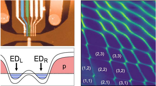
The first demonstration of graphene double quantum dots in which it
is possible to control the number of electrons down to zero has been
reported in Nano Letters. Far from an abstract academic stunt,
the results could prove key to future implementations of quantum
computing based on graphene. “Having exact information and control over
the number of electrons in the dots is essential for spin based quantum
information technology,” says Luca Banszerus, a researcher at RWTH
Aachen University in Germany and the first author of the paper reporting
these results.
Although this level of control has been demonstrated in single quantum dots, this is the first demonstration in graphene double quantum dots,
which are particularly useful as spin qubits. “Using a double dot
heavily facilitates the readout of the electron’s spin state and the
implementation of quantum gates,” Banszerus adds.
Less edgy quantum dots
The idea of using graphene in quantum dots dates back almost as far
as the first reports of the material’s isolation in 2004. Graphene has
almost no spin-orbit interaction and very little hyperfine coupling,
which would suggest that spin lifetimes can be extremely high.
Unfortunately, quantum dots physically etched from larger graphene
flakes run into problems due to the disorder at the dot’s edges
disrupting the material’s behavior. As a result, the transport behavior
of these quantum dots is dominated by localized states at the edges.
“This leads to an unknown effective quantum dot size and an occupation
of typically many electrons,” says Banszerus.
Instead, Banszerus and colleagues at RWTH Aachen and the National Institute of Materials Science in Japan work with bilayer graphene,
which can be tuned to be a semiconductor. A voltage applied to specific
regions of a bilayer graphene flake can switch those regions to behave
as insulators, electrostatically defining a quantum dot that has no edge
states nearby.
The Aachen researchers strip single flakes of bilayer graphene from
graphite (mechanical exfoliation) and handle it using a dry pick-up
technique that hinges on van der Waals interactions. They encapsulate
the bilayer graphene in hexagonal boron nitride (hBN) crystal. They then
place the structure on a graphite flake, which acts as the bottom
electrode, and add chromium and gold split gates and finger gates
separated from the split gates by a 30-nm-thick layer of atomic layer
deposited Al2O3.
They were able to control the number of electrons on the quantum dots
by applying a voltage, which also affected the tunneling coupling
between the dots. As a result, once the total occupation of the two
quantum dots exceeds eight electrons, they begin to behave as one single
quantum dot, rather than a double quantum dot. Transport measurements
also revealed that the number of electrons loaded on the quantum dot
could be controlled down to zero electrons.
The idea of defining quantum dots in bilayer graphene
electrostatically in this way is not new. However, although different
groups have attempted this approach since 2010, the process required
recently discovered tricks of the trade, such as better encapsulation in
hBN and the use of graphite flakes as gates to get a clean band gap.
Banszerus says these developments came as quite a surprise and revived
interest in graphene quantum dots in 2018. He hopes the capabilities
they have now demonstrated will further spark activity in this field.
Coupling control
“Even though being able to control the number of charges in a
graphene double dot is a huge step forward, there are still many
problems to be solved on the road toward spin-based quantum information technology in graphene,” says Banszerus. Next, he hopes to tackle the problem of controlling the coupling between the quantum dots and the reservoir, which he hopes to achieve by adding an additional layer of interdigitated finger gates on top.
Posted by AGORACOM
at 12:09 PM on Thursday, March 5th, 2020
SPONSOR: ZEN Graphene Solutions: An emerging advanced materials and graphene development company with a focus on new solutions using pure graphene and other two-dimensional materials. Our competitive advantage relies on the unique qualities of our multi-decade supply of precursor materials in the Albany Graphite Deposit. Independent labs in Japan, UK, Israel, USA and Canada confirm this. Click here for more information
An optical image of the graphene device (shown above as a square gold pad) on a silicon dioxide/silicon chip. Shining metal wires are connected to gold electrodes for electrical measurement. The tiny graphene device has a length and width of just one-tenth of a millimeter. (Credit: Guorui Chen/Berkeley Lab)
Berkeley Lab scientists tap into graphene’s hidden talent as an electrically tunable superconductor, insulator, and magnetic device for the advancement of quantum information science
Ever since graphene’s discovery
in 2004, scientists have looked for ways to put this talented,
atomically thin 2D material to work. Thinner than a single strand of DNA
yet 200 times stronger than steel, graphene is an excellent conductor
of electricity and heat, and it can conform to any number of shapes,
from an ultrathin 2D sheet, to an electronic circuit.
Last year, a team of researchers led by Feng Wang, a faculty scientist in Berkeley Lab’s Materials Sciences Division and a professor of physics at UC Berkeley, developed a multitasking graphene device
that switches from a superconductor that efficiently conducts
electricity, to an insulator that resists the flow of electric current,
and back again to a superconductor.
Now, as reported in Nature today,
the researchers have tapped into their graphene system’s talent for
juggling not just two properties, but three: superconducting,
insulating, and a type of magnetism called ferromagnetism. The
multitasking device could make possible new physics experiments, such as
research in the pursuit of an electric circuit for faster,
next-generation electronics like quantum computing technologies.
Optical image of a trilayer graphene material sandwiched between
boron nitride layers during the nanofabrication process (left); and the
trilayer graphene/boron nitride device with gold electrodes (right).
(Credit: Guorui Chen/Berkeley Lab)
“So far, materials simultaneously showing superconducting,
insulating, and magnetic properties have been very rare. And most people
believed that it would be difficult to induce magnetism in graphene,
because it’s typically not magnetic. Our graphene system is the first to
combine all three properties in a single sample,†said Guorui Chen, a
postdoctoral researcher in Wang’s Ultrafast Nano-Optics Group at UC
Berkeley, and the study’s lead author.
Using electricity to turn on graphene’s hidden potential
Graphene has a lot of potential in the world of electronics. Its
atomically thin structure, combined with its robust electronic and
thermal conductivity, “could offer a unique advantage in the development
of next-generation electronics and memory storage devices,†said Chen,
who also worked as a postdoctoral researcher in Berkeley Lab’s Materials
Sciences Division at the time of the study.
The problem is that the magnetic materials used in electronics today
are made of ferromagnetic metals, such as iron or cobalt alloys.
Ferromagnetic materials, like the common bar magnet, have a north and a
south pole. When ferromagnetic materials are used to store data on a
computer’s hard disk, these poles point either up or down, representing
zeros and ones – called bits.
Graphene, however, is not made of a magnetic metal – it’s made of carbon.
So the scientists came up with a creative workaround.
By applying electrical voltages through the graphene device’s gates,
the force from the electricity prodded electrons in the device to circle
in the same direction, like tiny cars racing around a track. This
generated a forceful momentum that transformed the graphene device into a
ferromagnetic system.
More measurements revealed an astonishing new set of properties: The
graphene system’s interior had not only become magnetic but also
insulating; and despite the magnetism, its outer edges morphed into
channels of electronic current that move without resistance. Such
properties characterize a rare class of insulators known as Chern
insulators, the researchers said.
Even more surprising, calculations by co-author Ya-Hui Zhang of the
Massachusetts Institute of Technology revealed that the graphene device
has not just one, but two conductive edges, making it the first observed
“high-order Chern insulator,†a consequence of the strong
electron-electron interactions in the trilayer graphene.
Scientists have been in hot pursuit of Chern insulators in a field of
research known as topology, which investigates exotic states of matter.
Chern insulators offer potential new ways to manipulate information in a
quantum computer, where data is stored in quantum bits, or qubits. A
qubit can represent a one, a zero, or a state in which it is both a one
and a zero at the same time.
“Our discovery demonstrates that graphene is an ideal platform for
studying different physics, ranging from single-particle physics, to
superconductivity, and now topological physics to study quantum phases
of matter in 2D materials,†Chen said. “It’s exciting that we can now
explore new physics in a tiny device just 1 millionth of a millimeter
thick.â€
The researchers hope to conduct more experiments with their graphene
device to have a better understanding of how the Chern insulator/magnet
emerged, and the mechanics behind its unusual properties.
Researchers from Berkeley Lab; UC Berkeley; Stanford University; SLAC
National Accelerator Laboratory; Massachusetts Institute of Technology;
China’s Shanghai Jiao Tong University, Collaborative Innovation Center
of Advanced Microstructures, and Fudan University; and Japan’s National
Institute for Materials Science participated in the work.
Founded in 1931 on the belief that the biggest scientific challenges are best addressed by teams, Lawrence Berkeley National Laboratory
and its scientists have been recognized with 13 Nobel Prizes. Today,
Berkeley Lab researchers develop sustainable energy and environmental
solutions, create useful new materials, advance the frontiers of
computing, and probe the mysteries of life, matter, and the universe.
Scientists from around the world rely on the Lab’s facilities for their
own discovery science. Berkeley Lab is a multiprogram national
laboratory, managed by the University of California for the U.S.
Department of Energy’s Office of Science.
DOE’s Office of Science is the single largest supporter of basic
research in the physical sciences in the United States, and is working
to address some of the most pressing challenges of our time. For more
information, please visit energy.gov/science.