Posted by AGORACOM
at 3:36 PM on Wednesday, March 11th, 2020
SPONSOR: Lomiko Metals is focused on the exploration and development of minerals for the new green economy such as lithium and graphite. Lomiko owns 80% of the high-grade La Loutre graphite Property, Lac Des Iles Graphite Property and the 100% owned Quatre Milles Graphite Property. Lomiko is uniquely poised to supply the growing EV battery market. Click Here For More Information
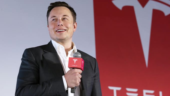
Tesla shares dropped by over 13% yesterday, amid continuing concerns
about the coronavirus outbreak and a steep drop in oil prices.
Musk’s announcement comes at a time when several large automakers are making moves into the electric vehicle sector.
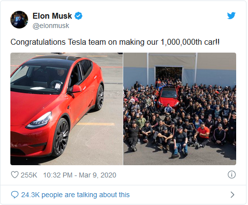
Tesla has
produced 1 million electric vehicles, according to the firm’s CEO Elon
Musk, who congratulated the “Tesla team†on the milestone via a tweet.
News of the landmark figure came after Tesla shares dropped by over 13% yesterday,
amid continuing concerns about the coronavirus outbreak and a steep
drop in oil prices. The Nasdaq Composite index, on which Tesla is
listed, fell 7.3 percent on the day. In extended hours trading Tuesday,
Tesla shares were over 10% higher
Currently, Tesla offers four models of electric vehicle: the Model 3
and Model S, which are sedans, and the Model Y and Model X, which are
types of SUV. Deliveries of the Model Y are due to start by the end of
this quarter.
Musk’s announcement comes at a time when several large automakers are making moves into the electric vehicle sector.
Towards the end of last year, the German company announced that 500,000 of its electrified cars had been sold.
At the time, CEO Oliver Zipse said that the business “was stepping up
the pace significantly†and aiming to have one million electric vehicles
on the road “within two years.â€
China’s electric car market is the biggest on the planet: a little
over one million electric cars were sold there in 2018, according to the
IEA, with Europe and the U.S. following behind.
Posted by AGORACOM
at 2:34 PM on Thursday, March 5th, 2020
SPONSOR: Lomiko Metals is focused on the exploration and development of minerals for the new green economy such as lithium and graphite. Lomiko owns 80% of the high-grade La Loutre graphite Property, Lac Des Iles Graphite Property and the 100% owned Quatre Milles Graphite Property. Lomiko is uniquely poised to supply the growing EV battery market. Click Here For More Information
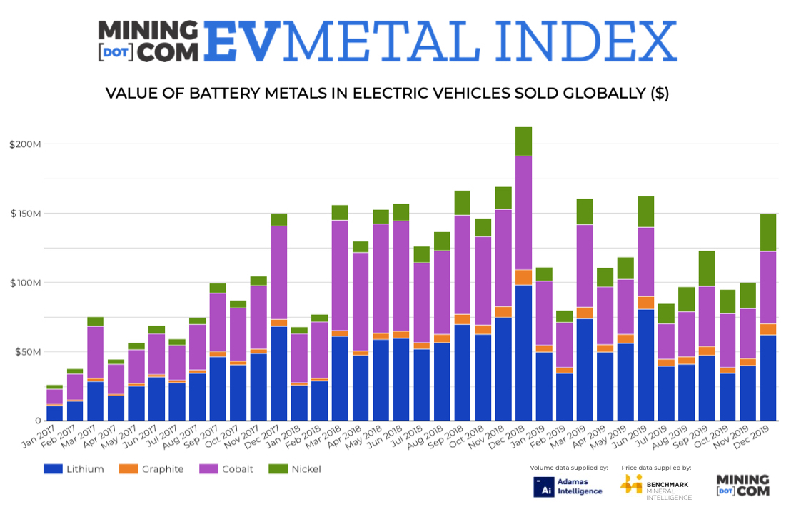
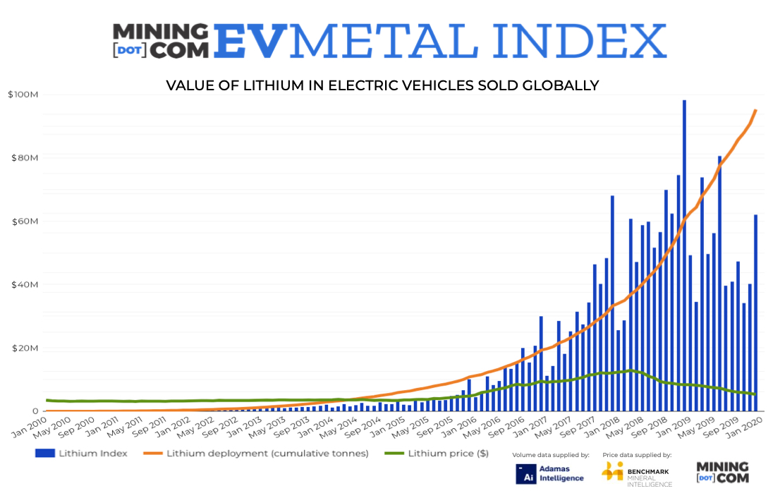
The value of metals used in batteries for the nascent electric vehicle industry measured for the first time
It is worth remembering that the first all-electric vehicle to use a
lithium-ion battery – the Tesla roadster – only rolled off assembly
lines in 2008.
And the blue-sky scenarios and exuberant forecasts for electric
vehicle demand and mining only really started to make headlines three or
four years ago.
And those headlines came just at the right time for an industry at
the bottom of a brutal business cycle and in desperate need of a
feelgood news story.
Not that the feeling lasted all that long.
All of mining is mercifully free of the ravages of price stability, but even tulip bulbs took longer from boom to bust than EV metals.
But how does falling prices for lithium, cobalt, graphite and nickel
square with demand forecasts that all start in the bottom left corner
and end in the top right?
Pedal to the metal
To get a better grip on the nascent sector, MINING.COM combined two sets of data:
First, prices paid for the mined minerals at the point of entry into the global battery supply chain.
London-based Benchmark Mineral Intelligence,
a global battery supply chain, megafactory tracker and market
forecaster, provides MINING.COM with monthly sales-weighted price data.
Second, the sales weighted volume of the raw materials in electric and hybrid passenger car batteries sold around the world.
Toronto-based Adamas Intelligence,
which tracks demand for EV batteries by chemistry, cell supplier and
capacity in over 90 countries provides the data for the raw materials
deployed.
Benchmark has been tracking megafactory construction since Tesla
broke ground on the first of its kind in June 2014. Adamas completes the
chain, recording all that battery power hitting the road.
That makes the MINING.COM EV Metals index more than a mine to market measure. More like mine to, er, garage.
The inaugural MINING.COM EV Metals Index shows an industry in better
shape than what tanking prices and dismal headlines would suggest.
In fact, the nickel sub-index is at a record high and cobalt bulls
would be happy to know that the metal feeding the battery supply chain
had its biggest month in nine.
If you take Tesla’s stock price as a guide (and I know a bunch of
short sellers who would rather pluck their own eyes out than do that)
the essential ingredients of muskmobiles should not be languishing at multi-year lows.
Last year, Elon Musk said getting more Teslas on the road is
dependent on scaling battery production and to scale at the fastest rate
possible it may be necessary to get into mining, “at least a little bit.â€
The last auto exec to venture into mining was Henry Ford
The last auto exec to venture into mining was Henry Ford. When the
equivalent of an over the air update was a hand crank and cars could
only be had in black and not four (wow!) other colours like the Model
S.
Crucially, at the time the cost of raw materials had a much bigger
bearing on the final price of a car. In EV production the battery can be
up to 50% of the cost of production and raw materials the bulk of
that.
A seminal study on EVs by UBS showed the only commodity your average
EV (Chevy Bolt) and ICE car (VW Golf) have in equal amounts, is rubber.
(Ford, btw, also owned a rubber plantation in Brazil.)
That’s how much of a change the switch to electric vehicles represents in the auto industry’s raw material supply chain.
Rocks down to electric avenue
Yet here we are.
Newbie investors are taking a crash course in surviving a sector that can turn on a dime.
Juniors are being scared off. Bodies are piling up among developers.
Producers’ grand ambitions have been thwarted. Contracts have been
reneged on.
It’s difficult to see the disconnect on fundamentals lasting that
much longer – governments’ green demands and emissions strictures are
only intensifying and carmakers’ programs are only becoming more
lavish.
Volkswagen promises 80 all electric models across its brands by 2025. Three hundred by the end of the decade.
While miners are encountering the pitfalls of vertical integration,
the global auto industry is getting a crash course in mining lead times
A year ago already, Wolfsburg said it was allocating $48 billion for EV development.
And then you also read that Audi (a VW brand) and Mercedes Benz had
to suspend production due to a battery shortage (long before
coronavirus).
While miners are encountering the pitfalls of vertical integration,
the global auto industry is getting a crash course in mining lead times
and how tiny markets (annual global cobalt mining revenue is less than
what VW collects in a week) can impact giant industries.
In total, the world’s automakers have committed $300 billion for
making rides you have to plug into a wall, Benchmark estimates. Or to
use the car industry term, $300 billion for ushering in a new epoch of
sustainable mobility.
Neither is there a shortage of government support for the transition. Unlike AOC’s,
the EU’s $1 trillion green new deal may actually get off the starting
grid, and Beijing has ordered 25% of cars sold must be EVs within five
short years.
Lithium nirvana
MINING.COM compiled the data for lithium prices from Benchmark and lithium deployment from Adamas going back eleven years.
It just shows again that the EV raw materials industry is in its infancy.
For calendar year 2009, the electric and hybrid cars sold around the
world contained a paltry 31 tonnes of lithium in their batteries worth a
combined $182K (that’s a K not an m).
Eleven years later, the industry had grown 3,330-fold for a value of
$609m. Ok, that’s just having fun with the base effect, but measured
just over the last five years the annualized value of lithium in EVs are
up more than 1,000%.
And that’s despite a contraction in 2019. Lithium price tripled
between April 2015 and peaked three years later, only to tumble by 60%
in value since then.
Graphite was the first to peak in early 2012, but has since halved.
The value of graphite deployed in EVs is up 370% in three years. And as a
percentage of the index, graphite has in fact steadily increased its
share.
The bigger picture is one of an industry that is still expanding. And at a breakneck pace.
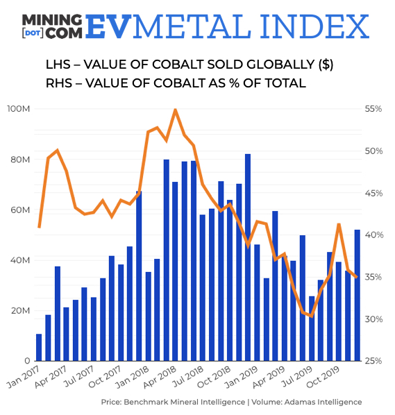
Cobalts from the blue
Given its tricky fundamentals, cobalt is always going to be a conundrum for investors and a headache for carmakers.
It’s the priciest component and the most volatile.
At its peak, Co made up as much as 55% of the cost of raw materials for
batteries. Despite a plummeting price and ongoing thrifting, it still
makes up a third of the input cost.
Given that almost two-thirds primary supply is from the Congo and
more than 80% of processing capacity is located in China, cobalt’s spike
to just shy of $110,000 a tonne in April 2018 was understandable.
That 15 months later it was below $26,000, less so.
At the stroke of a pen, Beijing can change market dynamics
completely. Its subsidy cuts last year crumpled a market growing at more
than 60% the year before.
In February, Tesla – which in good months sells more battery capacity than its three nearest rivals combined – surprised cobalt and nickel bulls by opting for batteries at its Shanghai plant that forego both.
At the time of writing, the impact of the four Cs –
cobalt-Congo-China-coronavirus – is far from clear. But as the graph
shows, cobalt bulls had something to celebrate in the second half of last year.
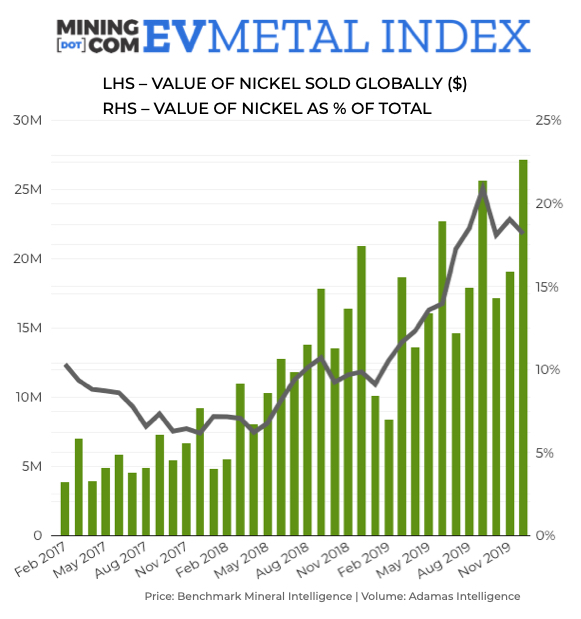
Better than the devil’s copper you know
Batteries account for only 6% of global nickel demand today, meaning
investors buying into the sulphates story also take a hit when Jakarta
convulses the nickel pig iron trade.
MINING.COM’s inaugural index shows nickel setting a new monthly record at the end of last year, despite the sharp retreat in prices since September.
The increasing use of nickel rich cathodes also means its
contribution to the value mix has almost doubled in a year to more than
18%.
As nickel-rich chemistries increasingly dominate the EV market, the
average sales weighted value of nickel on a per vehicle basis is rising
sharply – to over $100 in December from $67 a year earlier or from less
than a quarter of the cost of the cathode’s cobalt to half that.
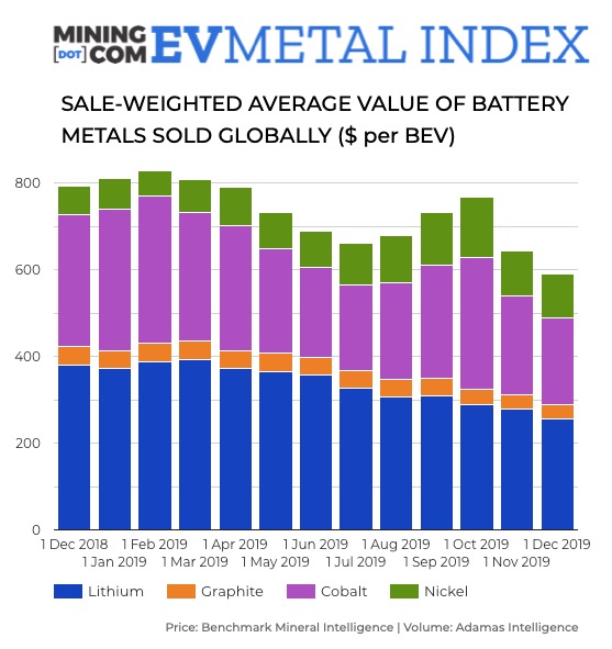
The combined value of lithium, graphite, cobalt and nickel based on sales weighted average deployed per vehicle was under $600.
When prices were peaking in early 2018 those raw materials cost more
than $1,500 per vehicle. Not the battery, just the raw materials.
In the longer run, nickel for batteries could be as big a market as
for stainless steel, which would be equivalent to gold’s use in
electronics, becoming a $100 billion industry, from an afterthought
today.
Kalahari thirst
Adamas data shows that NCM (nickel-cobalt-manganese) and NCA
(nickel-cobalt-aluminum) cathodes had a 94% market share in December,
based on total battery capacity deployed globally.
MINING.COM is not tracking manganese as EV dynamics have almost no bearing on its price.
High-purity manganese sulphate usually sells at a healthy premium,
but as a component of NCM batteries, no auto exec is losing sleep over
manganese costs or supply.
Likewise aluminum, despite significantly higher use in EVs.
That said, in an all-EV world battery-grade manganese demand could
make the Kalahari desert, home to the oldest population of humans on
earth and 70% of global reserves, a point of contention not unlike
cobalt and the Congo (minus the child labour and ongoing violent
conflict).
We lose money on every sale, but make it up on volume
Call them giga or mega, your average battery manufacturing plant is huge.
There are more than 100 megafactories in the pipeline around the world – 14 of them in Europe.
MINING.COM’s prediction is that 2019 wasn’t only the first annual fall in the index, but also the last
Last year battery power deployed rose 30% globally. In Europe, gigawatt hours hitting the road grew 89%.
To feed those factories to power those cars requires the extraction
of lithium, graphite, cobalt and nickel to increase by magnitudes.
The MINING.COM EV Metals Index shows that the gap between future supply and future demand has become a chasm.
MINING.COM’s prediction is that 2019 wasn’t only the first annual fall in the index, but also the last.
Posted by AGORACOM
at 12:09 PM on Thursday, March 5th, 2020
SPONSOR: ZEN Graphene Solutions: An emerging advanced materials and graphene development company with a focus on new solutions using pure graphene and other two-dimensional materials. Our competitive advantage relies on the unique qualities of our multi-decade supply of precursor materials in the Albany Graphite Deposit. Independent labs in Japan, UK, Israel, USA and Canada confirm this. Click here for more information
An optical image of the graphene device (shown above as a square gold pad) on a silicon dioxide/silicon chip. Shining metal wires are connected to gold electrodes for electrical measurement. The tiny graphene device has a length and width of just one-tenth of a millimeter. (Credit: Guorui Chen/Berkeley Lab)
Berkeley Lab scientists tap into graphene’s hidden talent as an electrically tunable superconductor, insulator, and magnetic device for the advancement of quantum information science
Ever since graphene’s discovery
in 2004, scientists have looked for ways to put this talented,
atomically thin 2D material to work. Thinner than a single strand of DNA
yet 200 times stronger than steel, graphene is an excellent conductor
of electricity and heat, and it can conform to any number of shapes,
from an ultrathin 2D sheet, to an electronic circuit.
Last year, a team of researchers led by Feng Wang, a faculty scientist in Berkeley Lab’s Materials Sciences Division and a professor of physics at UC Berkeley, developed a multitasking graphene device
that switches from a superconductor that efficiently conducts
electricity, to an insulator that resists the flow of electric current,
and back again to a superconductor.
Now, as reported in Nature today,
the researchers have tapped into their graphene system’s talent for
juggling not just two properties, but three: superconducting,
insulating, and a type of magnetism called ferromagnetism. The
multitasking device could make possible new physics experiments, such as
research in the pursuit of an electric circuit for faster,
next-generation electronics like quantum computing technologies.
Optical image of a trilayer graphene material sandwiched between
boron nitride layers during the nanofabrication process (left); and the
trilayer graphene/boron nitride device with gold electrodes (right).
(Credit: Guorui Chen/Berkeley Lab)
“So far, materials simultaneously showing superconducting,
insulating, and magnetic properties have been very rare. And most people
believed that it would be difficult to induce magnetism in graphene,
because it’s typically not magnetic. Our graphene system is the first to
combine all three properties in a single sample,†said Guorui Chen, a
postdoctoral researcher in Wang’s Ultrafast Nano-Optics Group at UC
Berkeley, and the study’s lead author.
Using electricity to turn on graphene’s hidden potential
Graphene has a lot of potential in the world of electronics. Its
atomically thin structure, combined with its robust electronic and
thermal conductivity, “could offer a unique advantage in the development
of next-generation electronics and memory storage devices,†said Chen,
who also worked as a postdoctoral researcher in Berkeley Lab’s Materials
Sciences Division at the time of the study.
The problem is that the magnetic materials used in electronics today
are made of ferromagnetic metals, such as iron or cobalt alloys.
Ferromagnetic materials, like the common bar magnet, have a north and a
south pole. When ferromagnetic materials are used to store data on a
computer’s hard disk, these poles point either up or down, representing
zeros and ones – called bits.
Graphene, however, is not made of a magnetic metal – it’s made of carbon.
So the scientists came up with a creative workaround.
By applying electrical voltages through the graphene device’s gates,
the force from the electricity prodded electrons in the device to circle
in the same direction, like tiny cars racing around a track. This
generated a forceful momentum that transformed the graphene device into a
ferromagnetic system.
More measurements revealed an astonishing new set of properties: The
graphene system’s interior had not only become magnetic but also
insulating; and despite the magnetism, its outer edges morphed into
channels of electronic current that move without resistance. Such
properties characterize a rare class of insulators known as Chern
insulators, the researchers said.
Even more surprising, calculations by co-author Ya-Hui Zhang of the
Massachusetts Institute of Technology revealed that the graphene device
has not just one, but two conductive edges, making it the first observed
“high-order Chern insulator,†a consequence of the strong
electron-electron interactions in the trilayer graphene.
Scientists have been in hot pursuit of Chern insulators in a field of
research known as topology, which investigates exotic states of matter.
Chern insulators offer potential new ways to manipulate information in a
quantum computer, where data is stored in quantum bits, or qubits. A
qubit can represent a one, a zero, or a state in which it is both a one
and a zero at the same time.
“Our discovery demonstrates that graphene is an ideal platform for
studying different physics, ranging from single-particle physics, to
superconductivity, and now topological physics to study quantum phases
of matter in 2D materials,†Chen said. “It’s exciting that we can now
explore new physics in a tiny device just 1 millionth of a millimeter
thick.â€
The researchers hope to conduct more experiments with their graphene
device to have a better understanding of how the Chern insulator/magnet
emerged, and the mechanics behind its unusual properties.
Researchers from Berkeley Lab; UC Berkeley; Stanford University; SLAC
National Accelerator Laboratory; Massachusetts Institute of Technology;
China’s Shanghai Jiao Tong University, Collaborative Innovation Center
of Advanced Microstructures, and Fudan University; and Japan’s National
Institute for Materials Science participated in the work.
Founded in 1931 on the belief that the biggest scientific challenges are best addressed by teams, Lawrence Berkeley National Laboratory
and its scientists have been recognized with 13 Nobel Prizes. Today,
Berkeley Lab researchers develop sustainable energy and environmental
solutions, create useful new materials, advance the frontiers of
computing, and probe the mysteries of life, matter, and the universe.
Scientists from around the world rely on the Lab’s facilities for their
own discovery science. Berkeley Lab is a multiprogram national
laboratory, managed by the University of California for the U.S.
Department of Energy’s Office of Science.
DOE’s Office of Science is the single largest supporter of basic
research in the physical sciences in the United States, and is working
to address some of the most pressing challenges of our time. For more
information, please visit energy.gov/science.
Posted by AGORACOM
at 9:53 AM on Monday, March 2nd, 2020
ZEN Graphene Solutions Ltd. (TSXV: ZEN) “ZEN” or the “Company“) is pleased to announce the launch of Albany Pure TM graphene products on their website at https://shop.zengraphene.com/.
The Company is planning to expand its product line to bring Graphene
Quantum Dots, Graphene Oxide, Reduced Graphene Oxide, and other
graphene-based products to the market.
The
Company is ramping up its new lab facility in Guelph, Ontario and is
working towards larger-scale graphene production. The graphene precursor
material is sourced from the unique, igneous-hosted Albany Graphite
Deposit in Northern Ontario. As part of the company’s business
development plan, ZEN is actively working with several industries to
functionalize and test its graphene products in their applications with
the potential for subsequent industry partnerships and agreements.
About ZEN Graphene Solutions Ltd.
ZEN
is an emerging graphene technology solutions company with a focus on
the development of graphene-based nanomaterial products and
applications. The unique Albany Graphite Project provides the company
with a potential competitive advantage in the graphene market as
independent labs in Japan, UK, Israel, USA and Canada have independently
demonstrated that ZEN’s Albany PureTM Graphite is an ideal precursor
material which easily converts (exfoliates) to graphene, using a variety
of mechanical, chemical and electrochemical methods.
Posted by AGORACOM
at 11:01 AM on Tuesday, February 25th, 2020
SPONSOR: ZEN Graphene Solutions: An emerging advanced materials and graphene development company with a focus on new solutions using pure graphene and other two-dimensional materials. Our competitive advantage relies on the unique qualities of our multi-decade supply of precursor materials in the Albany Graphite Deposit. Independent labs in Japan, UK, Israel, USA and Canada confirm this. Click here for more information
Researchers proposed a new design of the supercapacitor, which uses
films of graphene laminate with the same distance between the layers.
Energy density increases drastically — about 10 times compared to conventional supercapacitors.
Scientists from University College London and the Chinese Academy of Sciences have proposed a graphene-based design for supercapacitors, which reportedly increased their density by 10 times.
Supercapacitors charge quickly but also discharge at a high speed.
Existing supercapacitors tend to have a low energy density – about 1/20
of the battery capacity. Batteries
combined with supercapacitors are already in limited use – for example,
in Chinese public transport. But the bus in which such a battery is
installed is forced to charge at almost every stop.
In this work, the researchers proposed a new design of the
supercapacitor, which uses films of graphene laminate with the same
distance between the layers.
The work showed that when the pores in the membranes exactly
correspond to the size of the electrolyte ions, the energy density
increases drastically — about 10 times compared to conventional
supercapacitors.
In addition, the scientists note, the new material has a long service
life, retaining 97.8% of its energy intensity after 5000 cycles of
charging and discharging. The new supercapacitors are also very flexible
– they can be bent up to 180 degrees.
Posted by AGORACOM
at 9:27 AM on Tuesday, February 25th, 2020
SPONSOR: Lomiko Metals is focused on the exploration and development of minerals for the new green economy such as lithium and graphite. Lomiko owns 80% of the high-grade La Loutre graphite Property, Lac Des Iles Graphite Property and the 100% owned Quatre Milles Graphite Property. Lomiko is uniquely poised to supply the growing EV battery market. Click Here For More Information
TESLA REACHES $100 BILLION MARKET CAPITALIZATION WHILE MORGAN STANLEY PREDICTS $1200 LEVEL COMING SOON
Toronto, Ontario, Feb. 25, 2020 (GLOBE NEWSWIRE) — Lomiko Metals Inc. (“Lomikoâ€)
(TSX-V: LMR, OTC: LMRMF, FSE: DH8C) Lomiko Metals Inc. is pleased to
announce that the company will attend the Prospectors & Developers
Association Conference at the Metro Toronto Convention Centre March 1-4,
2020. Lomiko will be at booth #2547 in the Investors Exchange portion
of the Conference. Lomiko is focused on developing graphite materials
supply for the green economy.
Prospects for developing critical minerals mines in Quebec were
buoyed when Canada and the US announced January 9, 2020 they have
finalized the Canada-US Joint Action Plan on Critical Minerals
Collaboration. The Plan is aimed to secure a North American supply
chain for the critical minerals needed for manufacturing
sectors, communication technology, aerospace and defense, and clean
technology.
Canada has significant resources of graphite, lithium, cobalt, aluminum, and rare-earths.
Media has also focused on Tesla in recent interviews with CEO A. Paul
Gill who has consistently spoken about the coming change in consumer
purchasing patterns. In the last decade, range anxiety and concerns
over infrastructure have limited the penetration of electric vehicles in
the North American market and this has cast doubt on the potential of
Tesla. However, it is clear that those fears have been alleviated and
with the onset of new electric vehicles from Ford, GM, BMW, Audi,
Volkswagen, and others.
“Tesla stock price closing in on $ 1000 per share and its valuation
has exceeded $ 100 billion. This is a major indicator that investors
think electric vehicles will become mainstream. Every day, I see at
least one or more. And every time I see one, I think about the battery
it holds which contains up to 70 kgs of graphite.â€, stated A. Paul Gill,
CEO of Lomiko Metals, “That’s why Lomiko looked for projects with good
infrastructure, high grades, and high carbon purity so we could make
strides toward participating in the supply chain of electric vehicles
with materials such as spherical graphite and graphite anodes.â€
Mr. Gill has been interviewed on the Los Angles TV Show Big Biz and
the Geekery Review in Salt Lake City, Utah focusing on Tesla, EV
Batteries and Natural Flake Graphite.
Posted by AGORACOM
at 12:29 PM on Friday, February 21st, 2020
SPONSOR: Lomiko Metals is focused on the exploration and development of minerals for the new green economy such as lithium and graphite. Lomiko owns 80% of the high-grade La Loutre graphite Property, Lac Des Iles Graphite Property and the 100% owned Quatre Milles Graphite Property. Lomiko is uniquely poised to supply the growing EV battery market. Click Here For More Information
An Ivy charger on display at the 2020 Canadian International AutoShow in Toronto. Ontario Power Generation photo
Ivy Charging Network aims to create the “largest and most connected electric vehicle fast-charger network†in the province.
The company is expected to install 160 Level 3 fast-chargers at 73
locations across Ontario, each less than 100 kilometres apart from one
another on average, by the end of 2021.
Electric vehicle charging stations are coming to North Bay and
Temiskaming Shores as part of a new province-wide network being
developed by Hydro One and Ontario Power Generation (OPG).
Media releases from both Hydro One and OPG say they have launched a
new company, Ivy Charging Network, which aims to create the “largest and
most connected electric vehicle fast-charger network†in the province.
The company is expected to install 160 Level 3 fast-chargers at 73
locations across Ontario, each less than 100 kilometres apart from one
another on average, by the end of 2021.
Natural Resources Canada has provided an $8-million repayable
contribution, through its Electric Vehicle and Alternative Fuel
Infrastructure Deployment Initiative, to help build the network.
The Ivy Charging Network opened its first location in Huntsville in
September and an official public launch took place Friday at the 2020
Canadian International AutoShow in Toronto.
“We play a critical role in energizing life in communities across
Ontario. This fast-charger network will create a better and brighter
future through a greener transportation sector while meeting the
evolving energy needs of our customers and all Ontarians,†Hydro One
vice-president of customer service and Ivy Charging Network co-president
Imran Merali said.
“By entering this growing market in partnership with OPG, Hydro One
is expanding our product and service offering to deliver greater value
for our customers, employees, communities and shareholders.â€
Ivy Charging Network is a limited partnership owned equally by Hydro One and OPG.
The company has chosen Greenlots, a member of the Shell Group, as its service provider to operate and manage the network.
“Having delivered the world’s largest single climate change action to
date with the closure of our coal stations, OPG’s clean power serves as
a strong platform to electrify carbon-heavy sectors like
transportation,†fellow Ivy Charging Network co-president and OPG
vice-president of corporate business development and strategy Theresa
Dekker said.
“That’s why we’re so pleased to be partnering with Hydro One on an
initiative that will broaden the benefits of electrification and provide
a reliable, integrated network while ensuring no additional cost to
ratepayers.â€
Nipissing-Timiskaming Liberal MP Anthony Rota applauded the news on
Twitter, while Minister of Innovation, Science and Industry Navdeep
Bains said the federal government is committed to supporting projects
that will bring the country closer to a “competitive, zero-emissions
transportation sector.â€
He added that the network will ensure “Canadian-made solutions are at
the forefront of solving the global climate change crisis, leaving our
children and grandchildren with a healthier planet and cleaner air to
breathe.â€
Posted by AGORACOM
at 11:37 AM on Thursday, February 20th, 2020
SPONSOR: ZEN Graphene Solutions: An emerging advanced materials and graphene development company with a focus on new solutions using pure graphene and other two-dimensional materials. Our competitive advantage relies on the unique qualities of our multi-decade supply of precursor materials in the Albany Graphite Deposit. Independent labs in Japan, UK, Israel, USA and Canada confirm this. Click here for more information
Scientists at Rice University have made laser-induced graphene using a low-power laser mounted in a scanning electron microscope.
The team at Rice University,
in conjunction with Philip Rack, a Tennessee/ORNL materials scientist,
have pioneered a process to create laser-induced graphene (LIG). LIG has
features that are 60% smaller than the macro version of the material
and almost 10 times smaller than what can be typically achieved using an
infrared laser.
The LIG Process
LIG is a multifunctional graphene foam that is direct-written with an
infrared laser into a carbon-based precursor material. In the Rice
team’s research, this was achieved using a visible 405 nm laser that
directly converts polyimide into LIG, enabling the formation of LIG with
a spatial resolution of 12 µm and a thickness of < 5 µm. This
spatial resolution, enabled by the smaller-focused spot size of the 405
nm laser, represents a 60% reduction in previously reported LIG feature
sizes.
These smaller 405 nm lasers use light in the blue-violet part of the
spectrum. They are much less powerful than the industrial lasers that
are currently being used to burn graphene into materials.
“A key for electronics applications is to make smaller structures
so that one could have a higher density, or more devices per unit
area,†James Tour of Rice University said in a statement. “This method allows us to make structures that are 10 times denser than we formerly made.â€
A scanning electron microscope shows two tracers of LIG on a polyimide film. Image used courtesy of James Tour of Rice University
A New Path Toward Writing Electronic Circuits
To prove the viability of their concept, the researchers made tiny
flexible humidity sensors directly fabricated on polyimide. These
devices were then able to sense human breath in 250 milliseconds.
“This is much faster than the sampling rate for most commercial
humidity sensors and enables the monitoring of rapid local humidity
changes that can be caused by breathing,†said Rice postdoctoral researcher Michael Stanford, lead author of the research team’s paper.
The 405 nm laser is mounted on a scanning electron microscope (SEM)
and burns the top five microns of the polymer. This writes graphene
features as small as 12 microns.
The Rice team believes that this new LIG process could offer a new
path toward writing electronic circuits into flexible materials such as
clothing.
“The LIG process will allow graphene to be directly synthesized for precise electronics applications on surfaces,†added Stanford. With growing interest in the LIG process for use in flexible electronics and sensors, further refinement of this process will expand its utility and potentially see it being used in a range of flexible electronics across all industries.
Posted by AGORACOM
at 5:20 PM on Wednesday, February 19th, 2020
SPONSOR: Lomiko Metals is focused on the exploration and development of minerals for the new green economy such as lithium and graphite. Lomiko owns 80% of the high-grade La Loutre graphite Property, Lac Des Iles Graphite Property and the 100% owned Quatre Milles Graphite Property. Lomiko is uniquely poised to supply the growing EV battery market. Click Here For More Information
A. Paul Gill, CEO Lomiko Metals Inc. VP Business Development, appears on Michael Campbell’s MoneyTalks podcast, A financial show syndicated Canada-wide on the radio.
Posted by AGORACOM
at 6:40 PM on Friday, February 14th, 2020
SPONSOR: ZEN Graphene Solutions: An emerging advanced materials and graphene development company with a focus on new solutions using pure graphene and other two-dimensional materials. Our competitive advantage relies on the unique qualities of our multi-decade supply of precursor materials in the Albany Graphite Deposit. Independent labs in Japan, UK, Israel, USA and Canada confirm this. Click here for more information
Graphene has been dubbed the material of the future for its
unbelievable strength and the myriad of potential applications it offers
and European researchers have just released the first-ever manual on
how to produce it.
The manual was released by the Graphene Flagship consortium composed
of universities and companies. Founded in 2013, it is one of the three
big EU-funded science projects with a budget of over €1 billion until
2023.
The consortium hopes the manual will boost the uptake of the material which has the potential to revolutionise whole industries.
Graphene is a layer of carbon atoms obtained from graphite, which we can find, for example, in the tip of a pencil.
Arranged in a honeycomb-like pattern, it is 200 times stronger than
steel, harder than diamond, and carries both heat and electricity better
than any other material including gold or copper. And it’s also a
million times smaller than a strand of hair.
Seventy researchers participated in the elaboration of the free, 500-pages manual.
“It’s a big book that encompasses the description of many of the most
important methods to produce graphene and other two dimensional
materials,” Mar GarcÃa Hernández, from Graphene Flagship told Euronews.
Researchers from Graphene Flagship have shown that at least 1,800
different layered materials exit but so far, only a few have truly been
investigated.
“For any application of graphene or related materials, you need first
to be able to make it. For this reason, a book or a paper that gives
you precise details on how to make these materials, how to characterise
them, how to transfer them from the good substrate to the final
substrate is going to be very useful,” Andrea Ferrari, Graphene
Flagship’s Science and Technology Officer told Euronews.
The material’s flexibility and resilience mean it can be used in a
variety of industries such as aeronautics, space exploration, medicine,
energy or electronics.
Last December, Graphene Flagship
partnered with some of Europe’s biggest companies including Airbus,
Fiat-Chrysler Automobiles, Lufthansa Technik, Siemens and ABB among
others to take graphene-enabled prototypes to commercial applications.
One of the projects will develop state-of-the-art vision sensors,
which could be critical for the safe functioning of self-driving cars
while another will use graphene-based filters to remove contaminants
such as pesticides and dangerous pathogens from drinking water.