SPONSOR: Lomiko Metals LMR:TSX-V – A Canadian exploration-stage company discovered high-grade graphite at its La Loutre Property in Quebec and is working toward a Pre-Economic Assessment (PEA) that will increase its current indicated resource of 4.1 Mt of 6.5% Cg to over 10 Mt of 10%+ Cg through a 21 hole program at the Refractory Zone. Click Here For More Information
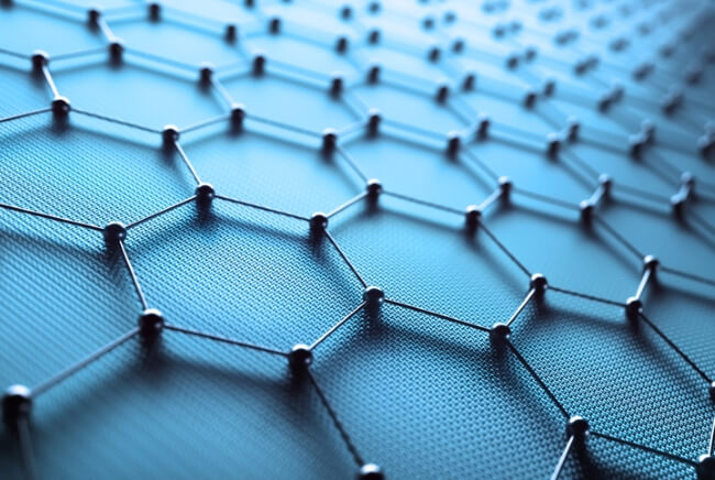
The emergence of graphene technology back in 2004 sent physicists and electronics engineers into euphoric spasms about its operational potential.
But as always with ground-breaking, technologies that old bean-counting devil called financial viability raised its head when it came to integrating graphene into commercial applications.
Challenges With Graphene
One of the problems during those pioneering days was the fact the graphene technology had so many varied and attractive properties and this meant it’s possible applications were numerous, to say the least.
However, in the enthusiastic rush to use the technology pragmatism took a back seat and some developers drastically overlooked the practical challenges in applying graphene to certain commercial areas.
But those days are disappearing and graphene is starting to fulfil its promises in a whole raft of applications from both technical and financial perspectives.
Graphene Technology Breakthroughs
More on those later but firstly let’s take a look at a couple of the latest and very exciting graphene breakthroughs that have a direct impact on the electronics industry. Over at the Danish funded Centre for Nanostructured Graphene at DTU and Aalborg University, researchers have finally cracked a well-known problem with graphene which focuses on how holes are made in the material.
This may sound simplistic but the pattern of holes dictates how the electrons in the material behave and this has direct relevance to how graphene can be designed into certain applications.
For years the nub of the problem has been that making the incredibly tiny nanoscale holes in graphene can cause contamination in the material which detrimentally alters its operational characteristics.
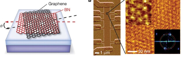
However, the team of scientists at the Centre have solved that problem by encapsulating the graphene inside another two-dimensional material, hexagonal boron nitride. This is a non-conductive material that can protect graphene’s properties.
Electron beam lithography was used to create the pattern in the protective layer of boron nitride and graphene. And to give you some idea of just how complex this work is the holes have a diameter of about 20 nanometres and there are only 12 nanometres space between them. Don’t forget, one nanometre is a billionth of a metre, or put another way a human hair is approximately 80,000 nanometres wide.
So why is this breakthrough such a big deal? One of the advantages of graphene is its potential application versatility, particularly in electronics but this versatility has until now been thwarted by the difficulty of introducing bandgap which is the difference between the top of the valence band, and the bottom of the conduction band.
We know that graphene is an incredibly good conductor but without an integral bandgap, it can’t be switched off which is an essential element in semiconductor-related applications. Now though, and thanks to this breakthrough, the bandgap problem has been overcome and in addition to that, the flow of electrical current through graphene has been increased a 1000-fold.
In another ground-breaking graphene development researchers at America’s Department of Energy’s Lawrence Berkeley National Laboratory have created a graphene device that easily switches from a superconducting material that conducts electricity without losing any energy, to an insulator that resists the flow of electric current, and back again to a superconductor.
The device consists of three nano-thin layers of graphene which are contained within layers of boron nitride and this forms a moiré superlattice pattern.
The researchers feel this material could help scientists further understand high-temperature superconductivity where material can conduct electricity without resistance at temperatures higher than expected, although these temperatures are still hundreds of degrees below freezing.
Innovations in Graphene Application Progress
So what about all those applications I mentioned earlier where graphene is starting to fulfil both its technical and financial promises?
Let’s start with batteries and energy storage products. With the environmental push towards electric vehicles (EVs), graphene can now help with lithium battery technology because it can reduce electrode resistance without decreasing active material content. This characteristic translates into batteries have increased performance at high discharge rates, something that designers of EVs like.
According to a report by IDTechEx Research graphene conductive inks are also becoming a reality. These had to prove that they offered both a performance and price advantage over carbon and metal-based products. However, these days graphene conductive inks are finding many applications in radio-frequency identification (RFID) antenna materials.
Graphene Uses
Graphene is also proving successful in thermal applications and is doing particularly well as a thermal spreader in cell phones. It provides much better thermal conductivity to copper at a lower weight.
SOURCE: https://www.electropages.com/blog/2019/08/Graphene-Technology-Finally-Grows-Up
Tags: #Battery, #High-Grade, #Ion, #Quebec, EV, lithium], Lomiko