Posted by AGORACOM-JC
at 8:06 PM on Sunday, July 19th, 2020
Lomiko Metals Inc.announced that it has engaged Kenmar Securities, LLC of New York (“The Advisor”) to raise $ 40 million Cdn for acquisition and development of critical metals projects. Kenmar Securities, LLC, is a Delaware limited liability corporation and SEC-registered securities broker-dealer and FINRA member.
The Advisor will assist the Company in analyzing its business, operations, properties, financial condition and prospects, prepare suitable marketing materials, contact any potential partner companies, assist and advise the Company with respect to the financial form and structure of any potential transaction.
“This year is the start of the Electric Vehicle Revolution. Lomiko would like to become part of the Battery Material supply chain” stated Mr. A. Paul Gill, CEO.
Posted by AGORACOM
at 6:23 PM on Friday, July 17th, 2020
Vancouver, B.C., July 17, 2020 (GLOBE NEWSWIRE) — Lomiko Metals Inc. (TSX-V: LMR, OTC: LMRMF, FSE: DH8C)(Lomiko or the “Company”) announces that it has engaged Kenmar Securities, LLC of New York (“The Advisor”) to raise $ 40 million Cdn for acquisition and development of critical metals projects. Kenmar Securities, LLC, is a Delaware limited liability corporation and SEC-registered securities broker-dealer and FINRA member.
The Advisor will assist the Company in analyzing its business, operations, properties, financial condition and prospects, prepare suitable marketing materials, contact any potential partner companies, assist and advise the Company with respect to the financial form and structure of any potential transaction.
“This year is the start of the Electric Vehicle Revolution. Lomiko would like to become part of the Battery Material supply chain” stated Mr. A. Paul Gill, CEO.
The Company agrees that, should the Company, or any affiliate of the Company, consummate any Transaction with a Referral pursuant to this Advisory Agreement, from the Effective Date through a period lasting until the twenty-four (24) month anniversary of the cancellation or termination of the Advisory Agreement, the Company shall pay to the Advisor, or cause the Advisor to be paid, at the funding of such Transaction, a success fee (the “Success Fee”) equivalent to five percent (5.0%) of the gross proceeds raised from the Transaction, which is equivalent to the total amount received or to be (and actually) received by the Company, from one or more Referrals. The Advisor cannot be certain that any amount of financing will be made available by its Referrals.
The payment of fees under any transaction is subject regulatory approval.
For more information on Lomiko Metals, review the website at www.lomiko.com, contact A. Paul Gill at 604-729-5312 or email: [email protected].
On Behalf of the Board,
“A. Paul Gill”
Chief Executive Officer
We seek safe harbor. Neither TSX Venture Exchange nor its Regulation Services Provider (as that term is defined in the policies of the TSX Venture Exchange) accepts responsibility for the adequacy or accuracy of this release
Posted by AGORACOM
at 11:17 AM on Tuesday, July 7th, 2020
SPONSOR: Lomiko Metals is focused on the exploration and development of minerals for the new green economy such as lithium and graphite. Lomiko has an option for 100% of the high-grade La Loutre graphite Property, Lac Des Iles Graphite Property and the 100% owned Quatre Milles Graphite Property. Lomiko is uniquely poised to supply the growing EV battery market. Click Here For More Information
Talking about batteries is just about as interesting as Scotch tape or paper clips. We take them for granted, but we all use them. Batteries have been around a long time. In 1938, archaeologists at a dig in Iraq uncovered the earliest -known battery dating back over 2000 years.
The first common, commercially available batteries like what we use today were invented in 1896 by a company that eventually renamed itself Eveready. These were specifically made for a new device called a “hand torch,†later known as a flashlight.
Fast-forward to today. The ubiquitous battery powers everything from watches to electric cars and solar power storage. It is found in satellites and home appliances, rockets and drones.
Electric vehicle batteries : range and MPGe
Batteries have had several key limitations, such as how long they hold a charge, how much power they can deliver on demand and how many charge cycles they can sustain. Let’s dive into one of the most recognizable battery applications, powering Tesla’s line of electric vehicles , known as EVs, and focus on range and how it compares to traditional mpg of gas-powered autos.
Tesla’s first production model car when introduced, the Roadster, had a battery capable of 200 miles per charge. Within a matter of months, with software updates and battery improvements, the EPA rated it at 244 miles on a single charge with 120 miles-per-gallon-equivalent. A total of 2,450 Roadsters were sold from 2008 through 2012.
The next vehicle, and the first high-volume production auto introduced in July 2012, was the Model S full-size sedan with sales totaling over 120,000 cars to date. The current Model S Long Range Plus has an EPA range of 402 miles and 104 MPGe.
The follow-up to the Model S was the Model X SUV, which began production in earnest in late 2015 with a total production to date of over 75,000. The battery in the Long Range Plus version has an EPA range of 351 miles with 94 MPGe.
Next up is Tesla’s Model 3, the most successful electric vehicle in history with more than 350,000 cars sold since its debut in 2017. It has an EPA rated range of 402 miles with 104 MPGe.
The Million Mile battery
Now the game-changer. Tesla has announced a battery upgrade that signals the death-knell for the internal combustion engine. Tesla worked with a Chinese battery company, CATL, to create (and patent) a battery design that can last for 1.24 million miles and a minimum of 16 years of lifespan. Compare that to current automakers with car battery warranties covering 60,000-150,000 miles for 3 to 8 years.
CATL is not prohibited from supplying the new battery to other EV manufacturers, which is a typical Elon Musk move who, in 2014, famously made all Tesla patents available to use. Elon’s goal is to shift the world away from fossil fuel use and to stay ahead of everyone else by out-innovating them.
Why are internal combustion engine vehicles now obsolete?
The most expensive part of an EV is the battery. The threshold for an EV to be price comparable with its non-EV competitors is to get a battery costing under $100 per kilowatt hour. We have now reached that milestone.
Larger batteries allow EV’s to go much further on a single charge, and this new battery should provide EVs with average ranges of 400 to 500 miles or more to start. This takes care of range limitations.
Larger batteries also allow for substantially faster charging. To get to a full charge on any EV battery, the first 50% charges up quickly, while the second half takes much longer. Larger batteries mean the first 50% provides more storage capacity which charges up quickly. Industry pundits expect the million-mile battery to charge up to 250 to 350 miles of range in as fast as 10 minutes.
An auto built to last
Tesla’s drive units and bodies for their mass-production models, such as the Model 3, were designed to last a million miles. Add the new million-mile battery and you have an EV as the first truly multi-generational auto, one that your grandkids will still be able to drive. EVs have a fraction of the moving parts that an internal combustion engine vehicle has, which makes EV’s orders of magnitude more reliable and longer lasting. EV batteries — for example, the ones used by Tesla’s Model S — currently last only 1,000 to 2,000 discharge cycles (a cycle is charging 0% to 100%), which is roughly 300,000 to 500,000 miles. The new million-mile battery is expected to hold more than 90% charge after 4,000 cycles. The average American driver clocks 13,476 miles a year. That translates to roughly 74 years of EV battery usage to reach a million miles.
The bottom line
Our current battle with COVID-19 did have one positive side effect, a drastic reduction in greenhouse gas emissions. China alone experienced a 25% reduction in carbon emissions and 50% reduction in nitrogen oxides emissions. Worldwide, daily carbon emissions during the lockdown in early April fell by 17% and could lead to an annual carbon emissions decline of up to 7%.
The tipping point for EVs vs. internal combustion engine vehicles is here. The dramatic cost reduction in solar, wind and hydro energy combined with EVs priced at or below internal combustion engine autos will finally lead to the world dumping its dependence on fossil fuels for power and transportation.
Technology advances will continue to drive down the cost of EVs, and solar/wind/hydro will do the same to electricity. Dump your gas-guzzling auto now for an electric vehicle before everyone figures out its value is about to plummet to scrap metal.
Posted by AGORACOM
at 4:03 PM on Wednesday, June 24th, 2020
SPONSOR: Lomiko Metals is focused on the exploration and development of minerals for the new green economy such as lithium and graphite. Lomiko has an option for 100% of the high-grade La Loutre graphite Property, Lac Des Iles Graphite Property and the 100% owned Quatre Milles Graphite Property. Lomiko is uniquely poised to supply the growing EV battery market. Click Here For More Information
The electric vehicle revolution has turned out to be more of an evolution, with the industry making slow and steady progress.
Despite this progress, the electric vehicle industry is still yet to turn a profit as a whole.
The next major step for the industry is to focus on efficiency and profitability, the two factors that will most impact the EV market share.
Many believe electric vehicles are the only future of road transportation. Equally, many are confident they will never replace internal combustion engines—not entirely, anyway. The so-called EV revolution, with sales of electric cars going through the roof and overtaking the sales of ICE cars, has failed to materialize. What the EV industry has instead been going through has been more stable and reliable: an evolution.
During this evolution, cutting battery costs and extending the range have been the two focal points of the EV industry. Now that there are some reliable results in these two respects, it is time to move to the next level: making EVs profitable.
It might come as a surprise that not all EVs are profitable, given that most EV-related headlines in the mainstream media are dedicated to Tesla, and Tesla continues to surprise the market with robust profits. But industry-wide, EVs have yet to turn in a profit, a new report from Lux Research says.
According to the report, the electric vehicle industry has made significant progress on battery costs and range extension, which has helped boost sales. Now, Lux Research analysts say, it is time to focus on efficiency to drive profitability, which would eventually make EVs more popular than ICE engine cars. This, the analysts say, should happen around 2035 or 2040, when plug-in hybrids and battery electric vehicles are expected to account for over half of all car sales.
“Currently, BEVs are more expensive and less convenient to use than their non-electric counterparts, but technology will continue to close this gap,” the lead author of the report, Christopher Robinson said. “We expect to see efficiency front and center as the next major focus of BEV design, with automakers either downsizing packs to increase profitability or offering more range.”
Naturally, the conclusions from the study are not based on research of every single EV that is on the global market. They are based on a representative sample of models, but, Robinson notes, there is a substantial difference between models in terms of profitability.
“Profitability in making electric vehicles ranges significantly between manufacturers. Tesla is likely the most profitable electric vehicle manufacturer with average gross margins around 20% on its vehicles,” the study’s lead author said. “However, that’s not the case for most as GM reported it still loses money on each Chevy Bolt it sells and has been hesitant to ramp up production. As incumbent manufacturers increase production capacity, we do expect profitability to improve through increased volumes of shared parts between models and advancements in batteries, motors, and other electronics in the powertrain.”
And then there are subsidies. Scorned by libertarians as a taxpayer-burdening crutch for industries that should be able to stand on their own two feet, subsidies for electric vehicles will remain in place for the observable future, at least in Europe and China, two of the world’s largest EV markets.
China recently said it would extend EV subsidies for two years, although it had planned to scrap them this year. It will gradually reduce them by 10 percent this year, 20 percent next year, and 30 percent in 2022, but it will keep them in place to stimulate more EV sales. Beijing has a target of 25 percent of all car sales to be EVs.
Meanwhile, Germany and France are even raising their EV subsidies to drive more purchases. These purchases are a big part of their green recovery plan, and in France, they are a big part of the revival of the local car industry, which has already invested heavily in electric vehicle manufacturing capabilities.
Sales of EVs this year will be affected by the pandemic, as will all car sales. BloombergNEF projects an 18-percent decline in EV sales this year but notes long-term demand remains strong.
Still, two more obstacles remain on the road to making EVs the dominant form of road transportation, and Lux Research analysts accurately call them range anxiety and charge time trauma. The reference to mental issues is not accidental. Besides their price, an inherent mistrust of EVs is a big reason why they are not a more common sight on roads and streets around the world.
Resolving these issues will take time, and they cannot be rushed, unless carmakers start handing out free EVs. After all, EVs are not an improvement on the ICE technology the way digital cameras were an improvement on analog ones. EVs are an alternative technology whose main advantage is that it does not emit noxious gases.
There are certainly many people concerned about the environment enough to be willing to spend more on a cleaner vehicle. Yet those who would rather keep their old truck, noxious gases and all, than buy an electric version and worry about charging times and ranges all the time are many more. These are the people whom the EV industry needs to convince that their product is reliable and won’t leave them stranded at a charging station in the middle of nowhere for hours.
Posted by AGORACOM
at 8:57 AM on Thursday, March 26th, 2020
Thunder Bay, Ontario–(March 26, 2020) – ZEN Graphene Solutions Ltd. (TSXV: ZEN) (“ZEN” or the “Company“)
has commenced scale-up and engineering studies on processes for the
production of Albany Pure ™ Graphene products at the Company’s research
and development facility in Guelph, Ontario. The priority is to increase
graphene production in anticipation of future demand as the Company
launched graphene product sales in early March 2020. ZEN will also
commission the recently purchased purification autoclave to commence the
production of high-purity Albany graphene precursor material.
ZEN’s graphene products will now all have the Albany Pure ™ Seal of
Authenticity which represents that the material was sourced from unique
Albany Graphite and meets the Company’s high-quality standards. Albany
Pure ™ Graphene products can be purchased online at
https://shop.zengraphene.com/.
The Company will be working with leading university researchers to
help facilitate the GO process scale-up at its Guelph facility. The
research and engineering team will also be developing and testing custom
functionalized graphene formulations as requested by industrial
collaborators for product performance enhancement.
The Company has also reviewed operational expenses and eliminated
non-core expenditures in response to the COVID-19 Pandemic and its
global economic fallout. This will ensure that scaled up graphene
production operations can move forward while the Company remains focused
on developing industrial partnerships. ZEN has also eliminated all
business-related air travel for employees as well as in-person meetings
until further notice.
About ZEN Graphene Solutions Ltd.
ZEN is an emerging graphene technology solutions company with a focus
on the development of graphene-based nanomaterial products and
applications. The unique Albany Graphite Project provides the company
with a potential competitive advantage in the graphene market as
independent labs in Japan, UK, Israel, USA and Canada have independently
demonstrated that ZEN’s Albany PureTM Graphite is an ideal precursor
material which easily converts (exfoliates) to graphene, using a variety
of mechanical, chemical and electrochemical methods.
To find out more on ZEN Graphene Solutions Ltd., please visit our website at www.ZENGraphene.com. A copy of this news release and all material documents in respect of the Company may be obtained on ZEN’s SEDAR profile at www.sedar.ca.
Posted by AGORACOM
at 11:07 AM on Thursday, March 12th, 2020
SPONSOR: ZEN Graphene Solutions: An emerging advanced materials and graphene development company with a focus on new solutions using pure graphene and other two-dimensional materials. Our competitive advantage relies on the unique qualities of our multi-decade supply of precursor materials in the Albany Graphite Deposit. Independent labs in Japan, UK, Israel, USA and Canada confirm this. Click here for more information
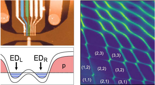
The first demonstration of graphene double quantum dots in which it
is possible to control the number of electrons down to zero has been
reported in Nano Letters. Far from an abstract academic stunt,
the results could prove key to future implementations of quantum
computing based on graphene. “Having exact information and control over
the number of electrons in the dots is essential for spin based quantum
information technology,” says Luca Banszerus, a researcher at RWTH
Aachen University in Germany and the first author of the paper reporting
these results.
Although this level of control has been demonstrated in single quantum dots, this is the first demonstration in graphene double quantum dots,
which are particularly useful as spin qubits. “Using a double dot
heavily facilitates the readout of the electron’s spin state and the
implementation of quantum gates,” Banszerus adds.
Less edgy quantum dots
The idea of using graphene in quantum dots dates back almost as far
as the first reports of the material’s isolation in 2004. Graphene has
almost no spin-orbit interaction and very little hyperfine coupling,
which would suggest that spin lifetimes can be extremely high.
Unfortunately, quantum dots physically etched from larger graphene
flakes run into problems due to the disorder at the dot’s edges
disrupting the material’s behavior. As a result, the transport behavior
of these quantum dots is dominated by localized states at the edges.
“This leads to an unknown effective quantum dot size and an occupation
of typically many electrons,” says Banszerus.
Instead, Banszerus and colleagues at RWTH Aachen and the National Institute of Materials Science in Japan work with bilayer graphene,
which can be tuned to be a semiconductor. A voltage applied to specific
regions of a bilayer graphene flake can switch those regions to behave
as insulators, electrostatically defining a quantum dot that has no edge
states nearby.
The Aachen researchers strip single flakes of bilayer graphene from
graphite (mechanical exfoliation) and handle it using a dry pick-up
technique that hinges on van der Waals interactions. They encapsulate
the bilayer graphene in hexagonal boron nitride (hBN) crystal. They then
place the structure on a graphite flake, which acts as the bottom
electrode, and add chromium and gold split gates and finger gates
separated from the split gates by a 30-nm-thick layer of atomic layer
deposited Al2O3.
They were able to control the number of electrons on the quantum dots
by applying a voltage, which also affected the tunneling coupling
between the dots. As a result, once the total occupation of the two
quantum dots exceeds eight electrons, they begin to behave as one single
quantum dot, rather than a double quantum dot. Transport measurements
also revealed that the number of electrons loaded on the quantum dot
could be controlled down to zero electrons.
The idea of defining quantum dots in bilayer graphene
electrostatically in this way is not new. However, although different
groups have attempted this approach since 2010, the process required
recently discovered tricks of the trade, such as better encapsulation in
hBN and the use of graphite flakes as gates to get a clean band gap.
Banszerus says these developments came as quite a surprise and revived
interest in graphene quantum dots in 2018. He hopes the capabilities
they have now demonstrated will further spark activity in this field.
Coupling control
“Even though being able to control the number of charges in a
graphene double dot is a huge step forward, there are still many
problems to be solved on the road toward spin-based quantum information technology in graphene,” says Banszerus. Next, he hopes to tackle the problem of controlling the coupling between the quantum dots and the reservoir, which he hopes to achieve by adding an additional layer of interdigitated finger gates on top.
Posted by AGORACOM
at 12:09 PM on Thursday, March 5th, 2020
SPONSOR: ZEN Graphene Solutions: An emerging advanced materials and graphene development company with a focus on new solutions using pure graphene and other two-dimensional materials. Our competitive advantage relies on the unique qualities of our multi-decade supply of precursor materials in the Albany Graphite Deposit. Independent labs in Japan, UK, Israel, USA and Canada confirm this. Click here for more information
An optical image of the graphene device (shown above as a square gold pad) on a silicon dioxide/silicon chip. Shining metal wires are connected to gold electrodes for electrical measurement. The tiny graphene device has a length and width of just one-tenth of a millimeter. (Credit: Guorui Chen/Berkeley Lab)
Berkeley Lab scientists tap into graphene’s hidden talent as an electrically tunable superconductor, insulator, and magnetic device for the advancement of quantum information science
Ever since graphene’s discovery
in 2004, scientists have looked for ways to put this talented,
atomically thin 2D material to work. Thinner than a single strand of DNA
yet 200 times stronger than steel, graphene is an excellent conductor
of electricity and heat, and it can conform to any number of shapes,
from an ultrathin 2D sheet, to an electronic circuit.
Last year, a team of researchers led by Feng Wang, a faculty scientist in Berkeley Lab’s Materials Sciences Division and a professor of physics at UC Berkeley, developed a multitasking graphene device
that switches from a superconductor that efficiently conducts
electricity, to an insulator that resists the flow of electric current,
and back again to a superconductor.
Now, as reported in Nature today,
the researchers have tapped into their graphene system’s talent for
juggling not just two properties, but three: superconducting,
insulating, and a type of magnetism called ferromagnetism. The
multitasking device could make possible new physics experiments, such as
research in the pursuit of an electric circuit for faster,
next-generation electronics like quantum computing technologies.
Optical image of a trilayer graphene material sandwiched between
boron nitride layers during the nanofabrication process (left); and the
trilayer graphene/boron nitride device with gold electrodes (right).
(Credit: Guorui Chen/Berkeley Lab)
“So far, materials simultaneously showing superconducting,
insulating, and magnetic properties have been very rare. And most people
believed that it would be difficult to induce magnetism in graphene,
because it’s typically not magnetic. Our graphene system is the first to
combine all three properties in a single sample,†said Guorui Chen, a
postdoctoral researcher in Wang’s Ultrafast Nano-Optics Group at UC
Berkeley, and the study’s lead author.
Using electricity to turn on graphene’s hidden potential
Graphene has a lot of potential in the world of electronics. Its
atomically thin structure, combined with its robust electronic and
thermal conductivity, “could offer a unique advantage in the development
of next-generation electronics and memory storage devices,†said Chen,
who also worked as a postdoctoral researcher in Berkeley Lab’s Materials
Sciences Division at the time of the study.
The problem is that the magnetic materials used in electronics today
are made of ferromagnetic metals, such as iron or cobalt alloys.
Ferromagnetic materials, like the common bar magnet, have a north and a
south pole. When ferromagnetic materials are used to store data on a
computer’s hard disk, these poles point either up or down, representing
zeros and ones – called bits.
Graphene, however, is not made of a magnetic metal – it’s made of carbon.
So the scientists came up with a creative workaround.
By applying electrical voltages through the graphene device’s gates,
the force from the electricity prodded electrons in the device to circle
in the same direction, like tiny cars racing around a track. This
generated a forceful momentum that transformed the graphene device into a
ferromagnetic system.
More measurements revealed an astonishing new set of properties: The
graphene system’s interior had not only become magnetic but also
insulating; and despite the magnetism, its outer edges morphed into
channels of electronic current that move without resistance. Such
properties characterize a rare class of insulators known as Chern
insulators, the researchers said.
Even more surprising, calculations by co-author Ya-Hui Zhang of the
Massachusetts Institute of Technology revealed that the graphene device
has not just one, but two conductive edges, making it the first observed
“high-order Chern insulator,†a consequence of the strong
electron-electron interactions in the trilayer graphene.
Scientists have been in hot pursuit of Chern insulators in a field of
research known as topology, which investigates exotic states of matter.
Chern insulators offer potential new ways to manipulate information in a
quantum computer, where data is stored in quantum bits, or qubits. A
qubit can represent a one, a zero, or a state in which it is both a one
and a zero at the same time.
“Our discovery demonstrates that graphene is an ideal platform for
studying different physics, ranging from single-particle physics, to
superconductivity, and now topological physics to study quantum phases
of matter in 2D materials,†Chen said. “It’s exciting that we can now
explore new physics in a tiny device just 1 millionth of a millimeter
thick.â€
The researchers hope to conduct more experiments with their graphene
device to have a better understanding of how the Chern insulator/magnet
emerged, and the mechanics behind its unusual properties.
Researchers from Berkeley Lab; UC Berkeley; Stanford University; SLAC
National Accelerator Laboratory; Massachusetts Institute of Technology;
China’s Shanghai Jiao Tong University, Collaborative Innovation Center
of Advanced Microstructures, and Fudan University; and Japan’s National
Institute for Materials Science participated in the work.
Founded in 1931 on the belief that the biggest scientific challenges are best addressed by teams, Lawrence Berkeley National Laboratory
and its scientists have been recognized with 13 Nobel Prizes. Today,
Berkeley Lab researchers develop sustainable energy and environmental
solutions, create useful new materials, advance the frontiers of
computing, and probe the mysteries of life, matter, and the universe.
Scientists from around the world rely on the Lab’s facilities for their
own discovery science. Berkeley Lab is a multiprogram national
laboratory, managed by the University of California for the U.S.
Department of Energy’s Office of Science.
DOE’s Office of Science is the single largest supporter of basic
research in the physical sciences in the United States, and is working
to address some of the most pressing challenges of our time. For more
information, please visit energy.gov/science.
Posted by AGORACOM
at 9:53 AM on Monday, March 2nd, 2020
ZEN Graphene Solutions Ltd. (TSXV: ZEN) “ZEN” or the “Company“) is pleased to announce the launch of Albany Pure TM graphene products on their website at https://shop.zengraphene.com/.
The Company is planning to expand its product line to bring Graphene
Quantum Dots, Graphene Oxide, Reduced Graphene Oxide, and other
graphene-based products to the market.
The
Company is ramping up its new lab facility in Guelph, Ontario and is
working towards larger-scale graphene production. The graphene precursor
material is sourced from the unique, igneous-hosted Albany Graphite
Deposit in Northern Ontario. As part of the company’s business
development plan, ZEN is actively working with several industries to
functionalize and test its graphene products in their applications with
the potential for subsequent industry partnerships and agreements.
About ZEN Graphene Solutions Ltd.
ZEN
is an emerging graphene technology solutions company with a focus on
the development of graphene-based nanomaterial products and
applications. The unique Albany Graphite Project provides the company
with a potential competitive advantage in the graphene market as
independent labs in Japan, UK, Israel, USA and Canada have independently
demonstrated that ZEN’s Albany PureTM Graphite is an ideal precursor
material which easily converts (exfoliates) to graphene, using a variety
of mechanical, chemical and electrochemical methods.
Posted by AGORACOM
at 11:01 AM on Tuesday, February 25th, 2020
SPONSOR: ZEN Graphene Solutions: An emerging advanced materials and graphene development company with a focus on new solutions using pure graphene and other two-dimensional materials. Our competitive advantage relies on the unique qualities of our multi-decade supply of precursor materials in the Albany Graphite Deposit. Independent labs in Japan, UK, Israel, USA and Canada confirm this. Click here for more information
Researchers proposed a new design of the supercapacitor, which uses
films of graphene laminate with the same distance between the layers.
Energy density increases drastically — about 10 times compared to conventional supercapacitors.
Scientists from University College London and the Chinese Academy of Sciences have proposed a graphene-based design for supercapacitors, which reportedly increased their density by 10 times.
Supercapacitors charge quickly but also discharge at a high speed.
Existing supercapacitors tend to have a low energy density – about 1/20
of the battery capacity. Batteries
combined with supercapacitors are already in limited use – for example,
in Chinese public transport. But the bus in which such a battery is
installed is forced to charge at almost every stop.
In this work, the researchers proposed a new design of the
supercapacitor, which uses films of graphene laminate with the same
distance between the layers.
The work showed that when the pores in the membranes exactly
correspond to the size of the electrolyte ions, the energy density
increases drastically — about 10 times compared to conventional
supercapacitors.
In addition, the scientists note, the new material has a long service
life, retaining 97.8% of its energy intensity after 5000 cycles of
charging and discharging. The new supercapacitors are also very flexible
– they can be bent up to 180 degrees.
Posted by AGORACOM
at 11:37 AM on Thursday, February 20th, 2020
SPONSOR: ZEN Graphene Solutions: An emerging advanced materials and graphene development company with a focus on new solutions using pure graphene and other two-dimensional materials. Our competitive advantage relies on the unique qualities of our multi-decade supply of precursor materials in the Albany Graphite Deposit. Independent labs in Japan, UK, Israel, USA and Canada confirm this. Click here for more information
Scientists at Rice University have made laser-induced graphene using a low-power laser mounted in a scanning electron microscope.
The team at Rice University,
in conjunction with Philip Rack, a Tennessee/ORNL materials scientist,
have pioneered a process to create laser-induced graphene (LIG). LIG has
features that are 60% smaller than the macro version of the material
and almost 10 times smaller than what can be typically achieved using an
infrared laser.
The LIG Process
LIG is a multifunctional graphene foam that is direct-written with an
infrared laser into a carbon-based precursor material. In the Rice
team’s research, this was achieved using a visible 405 nm laser that
directly converts polyimide into LIG, enabling the formation of LIG with
a spatial resolution of 12 µm and a thickness of < 5 µm. This
spatial resolution, enabled by the smaller-focused spot size of the 405
nm laser, represents a 60% reduction in previously reported LIG feature
sizes.
These smaller 405 nm lasers use light in the blue-violet part of the
spectrum. They are much less powerful than the industrial lasers that
are currently being used to burn graphene into materials.
“A key for electronics applications is to make smaller structures
so that one could have a higher density, or more devices per unit
area,†James Tour of Rice University said in a statement. “This method allows us to make structures that are 10 times denser than we formerly made.â€
A scanning electron microscope shows two tracers of LIG on a polyimide film. Image used courtesy of James Tour of Rice University
A New Path Toward Writing Electronic Circuits
To prove the viability of their concept, the researchers made tiny
flexible humidity sensors directly fabricated on polyimide. These
devices were then able to sense human breath in 250 milliseconds.
“This is much faster than the sampling rate for most commercial
humidity sensors and enables the monitoring of rapid local humidity
changes that can be caused by breathing,†said Rice postdoctoral researcher Michael Stanford, lead author of the research team’s paper.
The 405 nm laser is mounted on a scanning electron microscope (SEM)
and burns the top five microns of the polymer. This writes graphene
features as small as 12 microns.
The Rice team believes that this new LIG process could offer a new
path toward writing electronic circuits into flexible materials such as
clothing.
“The LIG process will allow graphene to be directly synthesized for precise electronics applications on surfaces,†added Stanford. With growing interest in the LIG process for use in flexible electronics and sensors, further refinement of this process will expand its utility and potentially see it being used in a range of flexible electronics across all industries.